This collection of FEEE (Fundamentals of Electrical & Electronic Engineering) MCQ and Short Questions is carefully compiled based on previous years’ questions of WBSCTE. It is designed to help polytechnic students understand the exam pattern, important topics, and frequently asked concepts.
UNIT-1
1. Which component opposes any change in current? a) Resistor b) Capacitor c) Inductor d) Diode -JAN 2022
Answer: c) Inductor
Explanation: According to Lenz’s Law, an inductor develops an induced electromotive force (EMF) that opposes the change in magnetic flux. Mathematically, , meaning the voltage across the inductor is proportional to the rate of change of current, effectively resisting any sudden variations.
2. In case of ideal current sources, they have ___________ a) zero internal resistance b) low value of voltage c) large value of current d) infinite internal resistance –JAN 2022
Answer: d) infinite internal resistance
Explanation: An ideal current source must provide a constant current regardless of the load connected to it. To ensure that no current is diverted internally, its internal resistance (connected in parallel) must be infinite ().
3. For a DC voltage, an inductor (a) is virtually a short circuit. (b) is an open circuit. (c) Depends on polarity. (d) Depends on voltage value. –NOV 2022
Answer: (a) is virtually a short circuit.
Explanation: In steady-state DC, the frequency is zero (f = 0). Since inductive reactance is , the reactance becomes zero. Therefore, the inductor offers no opposition to DC current and behaves like a short circuit (ideal wire).
4. Energy is stored by the capacitor in the form of ___________. -NOV 2022
Answer: Electrostatic Field.
Explanation: When a voltage is applied across the plates of a capacitor, an electric field is established between the plates. The energy stored is given by the formula .
5. If two capacitance of 10μF & 15 μF are connected in parallel then the equivalent capacitance will be _________ μF. -NOV 2022
Answer: 25 μF.
Explanation: For capacitors connected in parallel, the total capacitance is the sum of individual capacitances: . Therefore, 10 + 15 = 25 μF.
6. What is the frequency of a D.C signal? –NOV 2022
Answer: Zero (0 Hz).
Explanation: Frequency is defined as the number of cycles per second. Since a Direct Current (DC) signal maintains a constant magnitude and direction over time, it does not complete any cycles, making its frequency zero.
7. What is a dependent Source? –NOV 2022
Answer: A source whose output (voltage or current) is controlled by another voltage or current existing elsewhere in the circuit.
Explanation: Unlike independent sources, dependent (or controlled) sources are represented by diamond shapes and are categorised into four types: VCVS, VCCS, CCVS, and CCCS.
8. What do you mean by capacitance of a capacitor? What is its unit? -2023
Answer: Capacitance is the ability of a capacitor to store electric charge per unit of potential difference. Its SI unit is the Farad (F).
Explanation: It is defined by the ratio . One Farad is the capacitance of a conductor which has a potential of one volt when it carries a charge of one coulomb.
9. An ideal current source has (a) zero internal resistance (b) infinite internal resistance (c) low value of voltage (d) large value of current –2024
Answer: (b) infinite internal resistance
Explanation: High internal resistance ensures that the source current does not branch off internally, maintaining a constant flow to the external load. (Repeated from Jan 2022).
10. The resistance of a conductor increases if its (a) length increases (b) area of cross-section increases (c) length as well as area of cross-section increases (d) value of specific resistance is kept constant. –2024
Answer: (a) length increases
Explanation: Resistance follows the formula . Thus, R is directly proportional to the length (l) and inversely proportional to the cross-sectional area (A). Increasing length adds more collisions for electrons, increasing resistance.
11. A wire has resistance of 16Ω. It is bent in the form of a circle. The effective resistance between two points on any diameter of the circle is a) 32Ω, b) 16Ω, c) 8Ω, d) 4Ω –2025
Answer: d) 4Ω
Explanation: When the 16Ω wire is bent into a circle, a diameter divides it into two equal semicircular paths. Each path has a resistance of Ω. These two 8Ω paths are effectively in parallel. Thus, Ω.
12. If 110V is applied across 220V, 100W bulb, the power consumed by it will be a) 100W, b) 50W, c) 25W, d) 12.5W. –2025
Answer: c) 25W
Explanation: Resistance of the bulb is Ω. When 110V is applied, the new power consumed is W. Alternatively, since voltage is halved, power (which is ) becomes th of original.
13. A current of 10A enters a parallel combination of two resistances of 2Ω and 3Ω. Then the currents through resistances will be a) 4A and 6A, b) 6A and 4A, c) 2A and 8A, d) 5A and 5A –2025
Answer: b) 6A and 4A
Explanation: Using the Current Division Rule: A. A.
UNIT-2
1. The unit of magnetomotive force is- a) ampere-turn b) weber c) mho d) Maxwell -JAN 2022
Answer: a) ampere-turn
Explanation: Magnetomotive Force (MMF) is the product of the number of turns in a coil (N) and the current (I) flowing through it (). Hence, its practical unit is the Ampere-turn (AT).
2. The property of a material which opposes the creation of magnetic flux is called- a) permeability b) permittivity c) reluctance d) resistance -JAN 2022
Answer: c) reluctance
Explanation: Reluctance (S) in a magnetic circuit behaves exactly like resistance in an electric circuit. It opposes the setup of magnetic flux when an MMF is applied to the magnetic path.
3. The energy stored in a magnetic field is given by (L= self inductance, I= current)- a) b) c) d) -JAN 2022
Answer: a)
Explanation: Inductors store energy in the form of a magnetic field. The electrical work required to build up the current against the self-induced back EMF calculates exactly to .
4. Eddy current loss is directly proportional to (f= frequency , Bm = maximum flux density)- (a) f² and Bm² (b) f and Bm (c) f and Bm² (d) f² and Bm -JAN 2022
Answer: (a) f2 and Bm2
Explanation: The empirical equation for eddy current loss per unit volume is . This means the loss scales squarely with both the operating frequency (f2) and the peak flux density ().
5. The direction of induced emf is such that it will oppose the cause to which it is created, is related to _____ law of electromagnetic induction. (a) Faraday’s (b) Lenz’s (c) Ohm’s (d) Ampere’s -JAN 2022
Answer: (b) Lenz’s
Explanation: Faraday’s law determines the magnitude of the induced voltage, but Lenz’s Law dictates its direction. The negative sign in represents this fundamental rule of physical opposition.
6. Fleming’s Left hand rule gives the direction of ___________. -NOV 2022
Answer: Force (or mechanical motion) acting on a current-carrying conductor placed in a magnetic field.
Explanation: It is primarily used to understand the operation of electric motors, where electrical energy is transformed into mechanical force.
7. Conductance in Electric circuit is analogous to _________ in Magnetic Circuit. -NOV 2022
Answer: Permeance
Explanation: Conductance measures the ease with which electric current passes through a medium (). Similarly, permeance is the reciprocal of reluctance and measures the ease with which magnetic flux can be established (P = 1/S).
8. Weber is the unit of _____________. -NOV 2022
Answer: Magnetic flux ().
Explanation: One Weber (Wb) is defined as the amount of magnetic flux which, linking a circuit of one turn, produces an EMF of one volt if reduced to zero at a uniform rate in one second.
9. What is the unit of inductance? -NOV 2022
Answer: Henry (H).
Explanation: Inductance measures a coil’s capacity to induce a voltage. A coil has an inductance of 1 Henry if a current changing at the rate of 1 Ampere per second induces an electromotive force of 1 Volt across its terminals.
10. Energy stored by a coil is doubled when its current is increased by percent (a) 25 (b) 50.5 (c) 41.4 (d) 100. -2024
Answer: (c) 41.4
Explanation: Energy is proportional to the square of current (). If the new energy is , then , which leads to . The increase in current is 1.414 – 1 = 0.414 or 41.4%
11. A coil with 500 turns carries a current of 2 A. The value of MMF of the coil is (a) 20 AT (b) 200 AT (c) 1000 AT (d) 55 AT -2024
Answer: (c) 1000 AT
Explanation: .
12. The SI unit of reluctance is a) AT/Wb, b)AT/m, c) AT, d)N/Wb -2025
Answer: a) AT/Wb
Explanation: Reluctance is defined as . Since the unit of MMF is Ampere-turn (AT) and the unit of flux is Weber (Wb), the unit for reluctance is AT/Wb (also equivalent to Inverse Henry, ).
13. A magnetic circuit requires 800 AT to produce certain amount of magnetic flux. If the magnetizing coil of 100 turns has 5Ω resistance, the voltage to be applied to the exciting coil must be a) 40V, b) 20V, c) 10V, d) 5V -2025
Answer: a) 40V
Explanation: First find the required current: . Next, apply Ohm’s Law to calculate the matching voltage: .
UNIT-3
1. The duration of one cycle known as _______ a) waveform b) peak value c) instantaneous value d) period -JAN 2022
Answer: d) period
Explanation: One complete cycle of an alternating quantity takes a certain amount of time, which is called the time period (T).
2. The unit of inductive reactance is– (a) Henry (b) Farad (c) Ohm (d) Joule -JAN 2022
Answer: c) Ohm
Explanation: Inductive reactance is given by . Since it opposes current flow like resistance, its unit is Ohm (Ω).
3. In an ac circuit ‘VI sin θ’ represents- a) Active power b) Reactive power c) Apparent power d) True power -JAN 2022
Answer: b) Reactive power
Explanation: Reactive power is given by:
Its unit is VAR (Volt-Ampere Reactive).
4. When sinusoidal voltage is applied across a pure capacitor the current in the capacitor- a) lags applied voltage by 90° b) leads applied voltage by 90° c) is in phase with applied voltage d) is in phase opposition with applied voltage -JAN 2022
Answer: b) leads applied voltage by 90°
Explanation: In a purely capacitive circuit, current reaches its maximum value before voltage. Therefore, current leads voltage by 90°.
5. Peak factor for a sine wave is- a) 1 b) 1.414 c) 1.11 d) 2 -JAN 2022
Answer: b) 1.414
Explanation:
6. The maximum value of sine wave current is 100 A, the rms value of current in the circuit will be- a) 70.7 A b) 100 A c) 50 A d) 70.7 mA -JAN 2022
Answer: a) 70.7 A
Explanation:
7. The current through a series RLC circuit under resonance condition will be (a) V/R (b) V/XC (c) V/XL (d) none of these -NOV 2022
Answer: a) V/R
Explanation: At resonance,
So impedance becomes minimum and equal to resistance only.
8. Two sinusoidal emfs are given as and . The phase difference between the two quantities in degrees is a) 15 b) 45 c) 75 d) 30 -NOV 2022
Answer: c) 75
Explanation:
9. The time constant of a series R-C circuit is given by ___________. -NOV 2022
Answer:
Explanation: The time constant of an RC circuit is the product of resistance and capacitance.
Unit = second.
10. Define the term form factor. -NOV 2022
Answer: Form Factor is the ratio of RMS value to Average value of an alternating quantity.
For a sine wave:
11. Calculate the time period of a periodic signal whose frequency is 60Hz. -NOV 2022
Answer: second
12. What is the unit of reactive Power? -NOV 2022
Answer: VAR (Volt-Ampere Reactive)
Explanation: Reactive power is measured in VAR.
13. What is power factor? Write the value of power factor for purely resistive circuit. -2023
Answer: Power factor is the cosine of the phase angle between voltage and current.
For a purely resistive circuit:
Therefore, power factor = unity (1).
14. Inductive reactance of a coil of inductance 0.2 H at 50 Hz is (a) 62.8 Ω (b) 628 Ω (c) 0.2 Ω (d) 10Ω -2024
Answer: a) 62.8 Ω
15. The power factor of a purely resistive circuit is (a) zero (b) unity (c) lagging (d) leading. -2024
Answer: b) unity
Explanation: In a purely resistive circuit, voltage and current are in phase.cos0∘=1
Hence power factor is unity.
16. A sinusoidal voltage is represented by . Its rms value of voltage is (a) 141.4 V (b) 100 V (c) 87.92 V (d) 200 V -2024
Answer: b) 100 V
Explanation:
Maximum value,
17. Which of the following is a correct representation of peak value in an AC Circuit? a) RMS value / Peak factor b) RMS value × Form factor c) RMS value / Form factor d) RMS value × Peak factor -2025
Answer: d) RMS value × Peak factor
Explanation:
Therefore,
18. If the supply frequency increases, the value of inductive reactance a) decreases b) increases c) does not change d) becomes zero -2025
Answer: b) increases
Explanation:
Inductive reactance is directly proportional to frequency. Therefore, if frequency increases, inductive reactance also increases.
19. The advantage of star-connected AC supply system is that a) line current is equal to phase current, b) it is a simple arrangement, c) voltages at two levels can be used, d) phase sequence can easily be changed. -2025
Answer: c) voltages at two levels can be used
Explanation: In a star-connected system, both line voltage and phase voltage are available, allowing two different voltage levels to be used for different loads.
UNIT-4
1. Voltage per turn in both primary and secondary winding of a transformer is- a) high in high voltage winding b) low in low voltage winding c) same d) cannot determine -JAN 2022
Answer: c) same
Explanation:
In a transformer, voltage per turn is the same for both primary and secondary windings.
Therefore, the voltage induced per turn is equal in both windings.
2. A 10 KVA, 1100/400 V, 50 Hz single phase transformer has 100 turns in the secondary winding. The number of turns in primary winding is _____. (Fill in the blank) -JAN 2022
Answer: 275 turns
Explanation:
For a transformer,
Given,
Therefore,
Hence, the number of primary turns is 275 turns.
3. Direction of rotation of the motor armature/rotor can be determined by applying Fleming’s left hand rule .(True/False) -JAN 2022
Answer: True
Explanation:
Fleming’s Left Hand Rule is used to determine the direction of force or motion in an electric motor. Hence, it determines the direction of rotation of the armature or rotor.
4. Transformer ratings are given in :a) kVA b) HP c) kVAR d) kW -NOV 2022
Answer: a) kVA
Explanation:
Transformer rating depends on voltage and current, not on power factor.
Therefore, transformers are rated in kVA.
5. The flux in transformer core a) increases with load, (b) decreases with load, (c) remains constant irrespective of load, d) none of the above. -NOV 2022
Answer: c) remains constant irrespective of load
Explanation:
The core flux mainly depends on supply voltage and frequency.
Since voltage and frequency are normally constant, the flux remains nearly constant irrespective of load.
6. Which of the following does not change in a transformer? (a) Current (b) Voltage (c) Frequency (d) All of the above. -NOV 2022
Answer: c) Frequency
Explanation:
A transformer can change voltage and current levels, but the frequency remains unchanged.
For example, a 50 Hz input produces a 50 Hz output.
7. In an auto-transformer, power is transferred, through a) Conduction process only (b) Induction process only (c) Both conduction and induction processes (d) Mutual coupling. -NOV 2022
Answer: c) Both conduction and induction processes
Explanation:
In an autotransformer, a part of power is transferred directly through electrical connection and the remaining part through electromagnetic induction.
8. Transformer cores are laminated in order to____________. -NOV 2022
Answer: Reduce eddy current loss
Explanation:
Thin insulated laminations increase the resistance to circulating currents inside the core and reduce eddy current loss.
9. A motor converts electrical energy into ___________ energy. -NOV 2022
Answer: Mechanical energy
Explanation:
An electric motor converts electrical energy into mechanical energy in the form of rotational motion.
10. On which principle the transformer works? -NOV 2022
Answer: Mutual Induction
Explanation:
A transformer operates on the principle of mutual induction, where a changing magnetic flux in the primary winding induces emf in the secondary winding.
11. What type of DC Motor used in traction? -NOV 2022
Answer: DC Series Motor
Explanation:
DC series motors provide very high starting torque, making them suitable for electric traction applications such as trains and trams.
12. What do you mean by voltage transformation ratio of a transformer? -2023
Answer: Voltage transformation ratio is the ratio of secondary voltage to primary voltage.
Explanation:
It is represented by
Also,
where and are primary and secondary voltages, and and are primary and secondary turns respectively.
13. Voltage per turn in both primary and secondary windings of a transformer is (a) high in high voltage winding (b) low in low voltage winding (c) same (d) can’t be determined -2024
Answer: c) same
Explanation:
For an ideal transformer,
Hence, voltage per turn remains the same in both windings.
14. Transformer rating are given in (a) KVA (b) HP (c) KVAR (d) kW -2024
Answer: a) KVA
Explanation:
Transformer losses depend on voltage and current, not on power factor. Therefore transformer ratings are expressed in kVA.
15. A transformer transforms, a) Power b) Voltage c) current d) frequency -2024
Answer: b) Voltage
Explanation:
The primary function of a transformer is to step up or step down voltage while keeping the frequency unchanged.
16. Transformer core is assembled with laminated sheet so as to a) reduce hysteresis loss, b) eddy current loss, c) reduce copper loss, d) ensure good magnetic coupling between the windings. -2025
Answer: b) eddy current loss
Explanation:
Lamination breaks the path of circulating currents inside the core and thereby reduces eddy current losses.
17. Which of the following dc motor is used in Railway Electric Traction?-a) dc shunt motor b) dc series motor c) dc compound motor d) separately excited dc motor -2025
Answer: b) dc series motor
Explanation:
Railway traction requires very high starting torque. DC series motors provide the highest starting torque among DC motors and are therefore used in railway traction systems.
UNIT-5
1. A diode is a/an- a. bidirectional device b. unidirectional device c. both (a) and (b) d. none of the above – JAN 2022
Answer: (b) unidirectional device
Explanation: A diode allows current to flow mainly in one direction (forward bias) and blocks current in the opposite direction (reverse bias). Therefore, it is called a unidirectional device.
2. Free electrons in p type material – a. are majority carrier b. are minority carriers c. both (a) and (b) d. none of the above – JAN 2022
Answer: (b) are minority carriers
Explanation: In P-type semiconductor, holes are the majority carriers and free electrons are the minority carriers.
3. At absolute temperature an intrinsic semiconductor has- a) few free electrons b) few holes c) many holes and free electrons d) no holes and free electrons – JAN 2022
Answer: (d) no holes and free electrons
Explanation: At absolute zero temperature (0 K), there is no thermal energy available to break covalent bonds. Hence, no free electrons and no holes are present.
4. Rectifier is used to convert (a) DC signal to AC signal (b) AC signal to Pulsating DC signal (c) Reducing the amplitude of DC signal (d) Generation of AC signal – NOV 2022
Answer: (b) AC signal to Pulsating DC signal
Explanation: A rectifier converts alternating current (AC) into pulsating direct current (DC).
5. The number of valence electrons in the outermost shell of semiconductor are (a) 6 (b) 4 (c) 6 (d) 7 – NOV 2022
Answer: (b) 4
Explanation: Common semiconductor materials such as Silicon and Germanium have four valence electrons in their outermost shell.
6. The potential barrier of a silicon diode is (a) 0.3 V (b) 0.7 V (c) 1 V (d) 5V – NOV 2022
Answer: (b) 0.7 V
Explanation: The barrier potential of a silicon diode at room temperature is approximately 0.7 V.
7. FET is a ______ controlled device – NOV 2022
Answer: Voltage controlled device
Explanation: In a Field Effect Transistor (FET), the output current is controlled by the input voltage applied at the gate terminal.
8. The number of junctions in an NPN transistor are __________ – NOV 2022
Answer: 2
Explanation: An NPN transistor consists of two PN junctions: Emitter-Base junction and Collector-Base junction.
9. The majority charge carrier in n-type material is ____________ – NOV 2022
Answer: Electrons
Explanation: In N-type semiconductor, donor atoms contribute extra electrons. Therefore, electrons become the majority charge carriers.
10. If the reverse bias of gate in JFET is increased, the width of the conducting channel is _________ – NOV 2022
Answer: Decreased
Explanation: Increasing the reverse gate voltage widens the depletion region, which narrows the conducting channel.
11. Give two examples of insulating material – NOV 2022
Answer: Glass and Rubber
Explanation: Insulators do not allow electric current to pass through them easily. Glass and rubber are common insulating materials.
12. Why is doping done on Semiconductor? – NOV 2022
Answer: To increase conductivity.
Explanation: Doping introduces impurities into a pure semiconductor to increase the number of charge carriers and improve conductivity.
13. Name one doping material for creation of N-Type Semiconductor – NOV 2022
Answer: Phosphorus
Explanation: Pentavalent elements such as Phosphorus, Arsenic, and Antimony are used to create N-type semiconductors.
14. What are the types of Rectifier available? – NOV 2022
Answer: Half-wave Rectifier and Full-wave Rectifier.
Explanation: A half-wave rectifier uses only one half-cycle of AC input, while a full-wave rectifier uses both half-cycles.
15. When PN junction diode is in forward bias, by increasing the battery voltage (a) Circuit resistance increases (b) Current through P-N junction increases (c) Current through P-N junction decreases (d) None of the above happens – 2024
Answer: (b) Current through P-N junction increases
Explanation: Increasing the forward bias voltage reduces the barrier potential and allows more current to flow through the diode.
16. A diode is a/an (a) bidirectional device (b) unidirectional device (c) both (a) and (b) (d) none of the above – 2024
Answer: (b) unidirectional device
Explanation: A diode conducts current mainly in one direction and blocks it in the opposite direction.
17. Potential barrier at a p-n junction is established due to a) majority carriers, b) minority carriers, c) both (a) and (b), d) donor and acceptor ions – 2025
Answer: (d) donor and acceptor ions
Explanation: The potential barrier is formed due to the immobile positive donor ions and negative acceptor ions present in the depletion region.
18. In common emitter configuration, BJT acts as a a) voltage controlled voltage source b) current controlled voltage source c) voltage controlled current source d) current controlled current source – 2025
Answer: (d) current controlled current source
Explanation: In a BJT, the collector current is controlled by the base current. Therefore, in common emitter configuration, it behaves as a current controlled current source (CCCS).
UNIT-6
1. An ideal OP-AMP has the following characteristics- (Rin = input resistance, A = open loop gain, Rout = output resistance) a) Rin= ∞, A= ∞ and Rout = 0 b) Rin= 0, A= ∞ and Rout = 0 c) Rin= ∞, A= 0 and Rout = ∞ d) Rin= 0, A= ∞ and Rout = ∞ – JAN 2022
Answer: (a) Rin = ∞, A = ∞ and Rout = 0
Explanation: An ideal OP-AMP has infinite input resistance so that no current enters the input terminals, infinite open-loop gain for maximum amplification, and zero output resistance for ideal power transfer.
2. The expression of voltage gain in an inverting amplifier using ideal OP-AMP is (Rf = feedback resistance, Ri = input resistance)- a. –Rf/Ri b. Rf/Ri c. 1+Rf/Ri d. –(1+Rf/Ri) – JAN 2022
Answer: (a) –Rf/Ri
Explanation: The voltage gain of an ideal inverting amplifier is given by:
The negative sign indicates that the output is 180° out of phase with the input.
3. The expression of voltage gain in a non-inverting amplifier using ideal OP-AMP is (Rf = feedback resistance, Ri = input resistance)- a. –Rf/Ri b. Rf/Ri c. 1+Rf/Ri d. –(1+Rf/Ri) – JAN 2022
Answer: (c) 1 + Rf/Ri
Explanation: The voltage gain of an ideal non-inverting amplifier is given by:
The output is in phase with the input signal.
4. An ideal OP-AMP has the following characteristics- (Rin = input resistance, A = open loop gain, Rout = output resistance) a) Rin= ∞, A= ∞ and Rout = 0 b) Rin= 0, A= ∞ and Rout = 0 c) Rin= ∞, A= 0 and Rout = ∞ d) Rin= 0, A= ∞ and Rout = ∞ – NOV 2022
Answer: (a) Rin = ∞, A = ∞ and Rout = 0
Explanation: An ideal OP-AMP should have infinite input resistance, infinite gain, and zero output resistance.
5. The CMRR of an OP-Amp is the ratio of ___________. – NOV 2022
Answer: Differential gain to common-mode gain.
Explanation: CMRR (Common Mode Rejection Ratio) is the ratio of differential gain (Ad) to common-mode gain (Ac). A high CMRR means better rejection of unwanted common-mode signals.
6. Name the two input terminals of OP-AMP? – NOV 2022
Answer: Inverting terminal (–) and Non-inverting terminal (+)
Explanation: An OP-AMP has two input terminals. One is marked with a minus sign (–) called the inverting input and the other with a plus sign (+) called the non-inverting input.
7. An ideal OPAMP is an ideal (a) current controlled current source (b) current controlled voltage source (c) voltage controlled voltage source (d) voltage controlled current source – 2024
Answer: (c) voltage controlled voltage source
Explanation: The output voltage of an OP-AMP is controlled by the difference between its input voltages. Therefore, it acts as a voltage controlled voltage source (VCVS).
8. CMRR for an OP-AMP should be a) as large as possible b) close to zero c) close to unity d) as small as possible – 2025
Answer: (a) as large as possible
Explanation: A large CMRR means the OP-AMP can effectively reject common-mode signals such as noise and interference while amplifying only the desired differential signal.
UNIT-7
1. Which of these sets of logic gates are known as universal gates? a. XOR, NAND, OR b. OR, NOT, XOR c. NOR, NAND, XNOR d. NOR, NAND – JAN 2022
Answer: (d) NOR, NAND
Explanation: NAND and NOR gates are called universal gates because any logic gate or logical function can be implemented using only NAND gates or only NOR gates.
2. A digital circuit that can store only 1 bit information- a. NOR gate b. XOR gate c. Flip flop d. AND gate – JAN 2022
Answer: (c) Flip flop
Explanation: A flip-flop is a bistable device capable of storing one binary bit (0 or 1) of information.
3. The logical sum of two or more than two logical products is termed as a. OR operation b. POS c. SOP d. NAND operation – JAN 2022
Answer: (c) SOP
Explanation: SOP (Sum of Products) is a Boolean expression where multiple product terms are combined using OR operation.
4. When two input of a NAND gate is high, the output of the gate will be (a) High (b) Low (c) Toggle between high & low (d) none of above – NOV 2022
Answer: (b) Low
Explanation: A NAND gate gives a LOW output only when all its inputs are HIGH.
5. The number of flip flops required in a decade counter is a) 2 (b) 3 (c) 4 (d) 10 – NOV 2022
Answer: (c) 4
Explanation: A decade counter counts from 0 to 9 (10 states). Since 2⁴ = 16 ≥ 10, four flip-flops are required.
6. The maximum possible number of states in a ripple counter with 5 flip-flops is (a)32 (b) 15 (c) 10 (d) 5 – NOV 2022
Answer: (a) 32
Explanation: For an n-flip-flop counter, the maximum number of states is 2ⁿ. Therefore, for 5 flip-flops, the number of states is 2⁵ = 32.
7. A̅ + B̅ is equivalent to a) A + B b) A.B c) A̅.B̅ d) A̅ + B̅ – NOV 2022
Answer: (d) A̅ + B̅
Explanation: The given expression is already in its simplest form. None of the other options are equivalent to A̅ + B̅.
8. The output of AND gate will be HIGH only when both the input is ____________ – NOV 2022
Answer: HIGH (1)
Explanation: An AND gate produces a HIGH output only when all inputs are HIGH.
9. The full form of TTL is ____________ – NOV 2022
Answer: Transistor-Transistor Logic
Explanation: TTL is a logic family in which transistors are used for both logic operation and amplification.
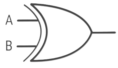
10. Draw the symbol of X-OR Gate – NOV 2022
11. Name any two types of Flip-Flop – NOV 2022
Answer: JK Flip-Flop and D Flip-Flop
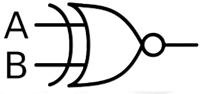
12. What is the full form of SOP and POS form of logic gates? Draw the symbol of two input Ex-NOR gate – 2023
Answer:
SOP = Sum of Products
POS = Product of Sums
Ex-NOR Gate Symbol:
13. When the two input of a NAND gate is high, the output of the gate will be (a) high (b) low (c) toggle between high & low (d) none of the above – 2024
Answer: (b) low
Explanation: A NAND gate produces LOW output only when all inputs are HIGH.
14. Which of these sets of logic gates are known as universal gates? (a) XOR, NAND, OR (b) OR, NOT, XOR (c) NOR, NAND, XNOR (d) NOR, NAND – 2024
Answer: (d) NOR, NAND
Explanation: NAND and NOR are universal gates because they can be used to realise all other logic gates.
15. If two inputs of a NOR gate is tied up, it will act as a a) NOT gate, b) OR gate, c) NAND gate, d) EX-NOR gate – 2025
Answer: (a) NOT gate
Explanation: If both inputs of a NOR gate are connected together, the output becomes the following:
Y = (A + A)̅ = A̅
Thus, the NOR gate behaves as a NOT gate.
16. A bulb in a stair-case has two switches… The logic of switching of the bulb resembles a) An AND gate, b) An OR gate, c) an XOR gate, d) A NAND gate – 2025
Answer: (c) an XOR gate
Explanation: In a staircase wiring system, the bulb turns ON when the two switch positions are different and turns OFF when they are the same. This behaviour is exactly the same as an XOR gate.